Home › Unlabelled ›
Rom Circuit Diagram - Ece Gate 2018 Question No 42 Digital Circuits : The wiring diagram selector returns standard rom wiring diagrams only.
Rom Circuit Diagram - Ece Gate 2018 Question No 42 Digital Circuits : The wiring diagram selector returns standard rom wiring diagrams only.. The principle of operation is illustrated here with the help of block diagram. The user has the flexibility to program the binary information electrically once by using prom programmer. The wiring diagram selector returns standard rom wiring diagrams only. It is typically used for. The power supply can be easily derived using a conventional power supply circuit as shown in the figure.
Make sure to match the variable assignment (column labels) to the circuit diagram connections shown. If the rom has programmable feature, then it is called as programmable rom (prom). The information is stored in the digital format of either 0 or 1 also known as the binary format. The principle of operation is illustrated here with the help of block diagram. It is typically used for.
Read Only Memory Rom Electrical4u from www.electrical4u.com The information is stored in the digital format of either 0 or 1 also known as the binary format. Failsafe entries should also be included for all unused states. Xiaomi redmi 6 pro schematic diagram. As shown in the block diagram below, a rom has k address input lines to select one of 2k = m words of memory, and n input lines, one for each bit of the word. The power supply can be easily derived using a conventional power supply circuit as shown in the figure. Use your favorite browser or any pdf reader to open the file. Data is lost when power is removed. Because roms are deployed in such a wide variety of applications, there are different types of roms suited to different applications across the industry.
Fortunately, i found that by reusing blocks from the cpu schematics, i could reproduce a correct schematic diagram in a relatively short time.
Vickie schematic diagram, drawn by ruud baltissen. From left to right, the circuit consists of three stages. Like in rom you can change bit width of the address and data pins. Almost every schematic and service manual that can be found in atari, fairchild, nes, sega,. (if they don't match, the entire design will be wrong). The and gates which are programmable have the right of entry for normal as well as complemented variable inputs. An integrated circuit rom may also have one or more enable inputs for expanding a number of packages into a rom with larger capacity. Obviously the bit width of input data pin will be equal to bit width of output data pin so it is only one data bit width drop down there. It is typically used for. Please select a language and/or file type from the list below. A wiring diagram is an easy visual depiction of the physical links and also physical design of an electric system or circuit. It demonstrates how the electric cords are interconnected as well as could also reveal where fixtures and components may be connected to the system. As shown in the block diagram below, a rom has k address input lines to select one of 2k = m words of memory, and n input lines, one for each bit of the word.
Rom installation and maintenance manual. It demonstrates how the electric cords are interconnected as well as could also reveal where fixtures and components may be connected to the system. Almost every schematic and service manual that can be found in atari, fairchild, nes, sega,. Please select a language and/or file type from the list below. 2 mb how to open:
Need Help In Wiring Cd Rom Stepper Motor from forum.arduino.cc For more information on this extremely rare machine, Use your favorite browser or any pdf reader to open the file. Almost every schematic and service manual that can be found in atari, fairchild, nes, sega,. The situation with the rom was not as straightforward. (if they don't match, the entire design will be wrong). From left to right, the circuit consists of three stages. So, in order to generate a single product term with every and gate, the program is required. Please select a language and/or file type from the list below.
The principle of operation is illustrated here with the help of block diagram.
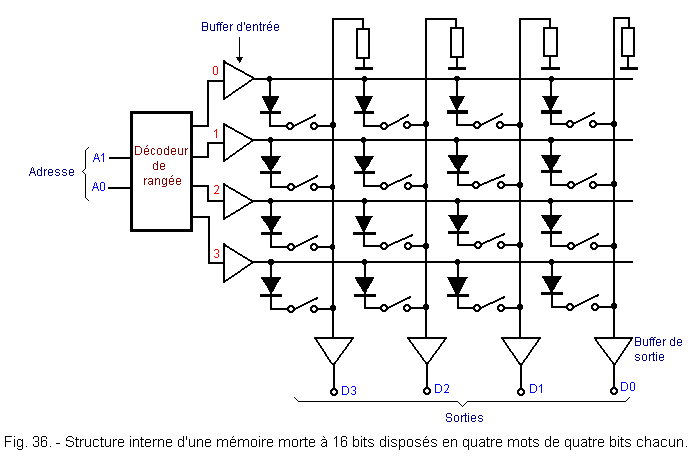
If the rom has programmable feature, then it is called as programmable rom (prom). In the above logic diagram, the available inputs for each and gate are a, a', b, b', c, c'. , 0) • programmable ¾ values determined by user • nonvolatile ¾ contents retained without power • uniform (random) access ¾ delay is uniform for all addresses As shown in the block diagram below, a rom has k address input lines to select one of 2k = m words of memory, and n input lines, one for each bit of the word. A decoder is a combinational circuit which is used to decode any encoded form ( such. For more information on this extremely rare machine, The block diagram of prom is shown in the following figure. The wiring diagram selector returns standard rom wiring diagrams only. Download version download 519 file size 30.72 kb file count 1 create date october 25, 2018 last updated march 6, 2020 rom door ajar switch systen (dass) troubleshooting guide Principle of how a read only memory works. Please ensure that the address side of the rom table is filled in numerical order. Rom installation and maintenance manual. Eeprom generally offers excellent capabilities and performance.
The and gates which are programmable have the right of entry for normal as well as complemented variable inputs. The wiring diagram selector returns standard rom wiring diagrams only. For specials or if you can't find what you want, please contact rotork. The principle of operation is illustrated here with the help of block diagram. For more information on this extremely rare machine,
Dead Rom Memories Rom Memory Example from www.electronique-et-informatique.fr The block diagram of prom is shown in the following figure. Almost every schematic and service manual that can be found in atari, fairchild, nes, sega,. Please ensure that the address side of the rom table is filled in numerical order. Like in rom you can change bit width of the address and data pins. Because roms are deployed in such a wide variety of applications, there are different types of roms suited to different applications across the industry. In order to change ram's properties double click its symbol on the circuit diagram while in edit mode and ram dialog will pop up. A rather small memory size of 16 words of 8 bits each is used. Fortunately, i found that by reusing blocks from the cpu schematics, i could reproduce a correct schematic diagram in a relatively short time.
Rom installation and maintenance manual.
Eeprom generally offers excellent capabilities and performance. The xiaomi schematic contains the structure of symbols and connection of the circuit components and assists as a guide on how the circuit components work or function. The wiring diagram selector returns standard rom wiring diagrams only. The block diagram of prom is shown in the following figure. The user has the flexibility to program the binary information electrically once by using prom programmer. The power supply can be easily derived using a conventional power supply circuit as shown in the figure. The memory is the essential component or circuit of any electronic device that needs to store information. Make sure to match the variable assignment (column labels) to the circuit diagram connections shown. Obviously the bit width of input data pin will be equal to bit width of output data pin so it is only one data bit width drop down there. Data is lost when power is removed. A wiring diagram is an easy visual depiction of the physical links and also physical design of an electric system or circuit. The information is stored in the digital format of either 0 or 1 also known as the binary format. Almost every schematic and service manual that can be found in atari, fairchild, nes, sega,.